
Periodic Morphologies via FIB induced Self-Organization and Site-Specific Defect Engineering on hBN
Bhaveshkumar Kamaliya (Tom Folland presenting)
McMaster University, Hamilton, Ontario, Canada _______________________________________
Focused Ion Beam (FIB) has been extensively used for direct milling for Nano- and Micro-structures. The foremost leverage using FIB, as compared to conventional lithography processes, for nanofabrication is that it is a mask-less (direct-writing) and single-step nanopatterning technique; however, it operates on a pixel-by-pixel dwelling, and the effective beam size of FIB restricts minimum feature size. Self-organization of the patterned surfaces and self-assembly effects induced by FIB-material interactions can be useful to fabricate unusual nanostructures with FIB, which are difficult or impossible to fabricate via conventional processes[1].
Here, we present self-organization (Figure 1) and local defect engineering (Figure 2) attempts on 2D van der Waals material, hexagonal Boron Nitride (hBN). Under focused ion beam (FIB irradiation, localized boron vacancies (V–B) or carbon substitutional defects (C0N & C0B) are created in hBN, resulting in photoluminescence at the patterned/irradiated regions[2,3]. Spectrally and spatially isolating the defects (e.g., boron vacancies vs carbon substitutional defects) is of prime interest due to distinct optical signals and their applicability as visible light single-photon sources. Here we present a pathway to create isolated defects induced by irradiating the hBN samples with varied ion species such as Xe+, Ne+ and He+ (Figure 2). In addition to this defect engineering, tuning the Xe+ PFIB (Plasma-FIB) irradiation parameters enables creating surface morphologies such as periodic nanoripples and nanopolygons (Figure 1) on the hBN surface via nanoscale-controlled surface self-organization. Hence, by controlling the pitch and morphology of self-organized structures, we fabricate grating-like hBN nanostructures, which also host quantum emitters, thereby realizing single-step fabrication of nanostructured quantum light sources. This defect engineering, in addition to controlled structural morphologies, provide the pathway towards unconventional optoelectronic devices and photonic properties.
[1] Kamaliya B, Garg V, Liu A C Y, Chen Y (Emily), Aslam M, Fu J and Mote R G 2021 Tailoring Surface Self-Organization for Nanoscale Polygonal Morphology on Germanium Adv. Mater. 33 2008668
[2] Kianinia M, White S, Fröch J E, Bradac C and Aharonovich I 2020 Generation of Spin Defects in Hexagonal Boron Nitride ACS Photonics 7 2147–52
[3] JLiu W, Guo N-J, Yu S, Meng Y, Li Z-P, Yang Y-Z, Wang Z-A, Zeng X-D, Xie L-K, Li Q, Wang J-F, Xu J-S, Wang Y-T, Tang J-S, Li C-F and Guo G-C 2022 Spin-active defects in hexagonal boron nitride Mater. Quantum. Technol. 2 032002
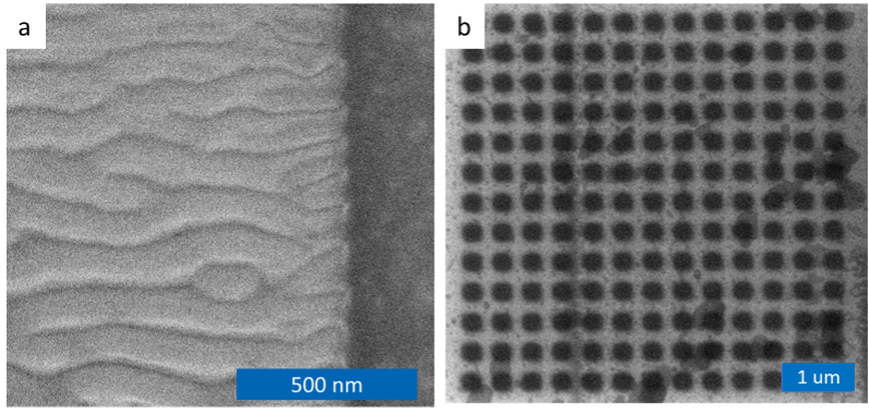
Figure 1.Xe+ PFIB irradiation induced nanoripples (a) and nanopolygons (b) on the hBN surface via surface self-organization.
 Figure 2.(a) PL emission from defects induced during nanoscale self-organization under Xe+ irradiation on hBN, (b) PL emission from defects induced under He+ irradiation on hBN, and (c) He+ ion irradiation produces intense PL from Boron vacancies while Xe+ irradiation led to the emission from Boron vacancies as well as Carbon defects. Ne+ irradiation does not lead to any PL response.
Email: bhaveshk@mcmaster.ca